
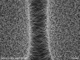
On-chip plasmonic-waveguide nanolaser
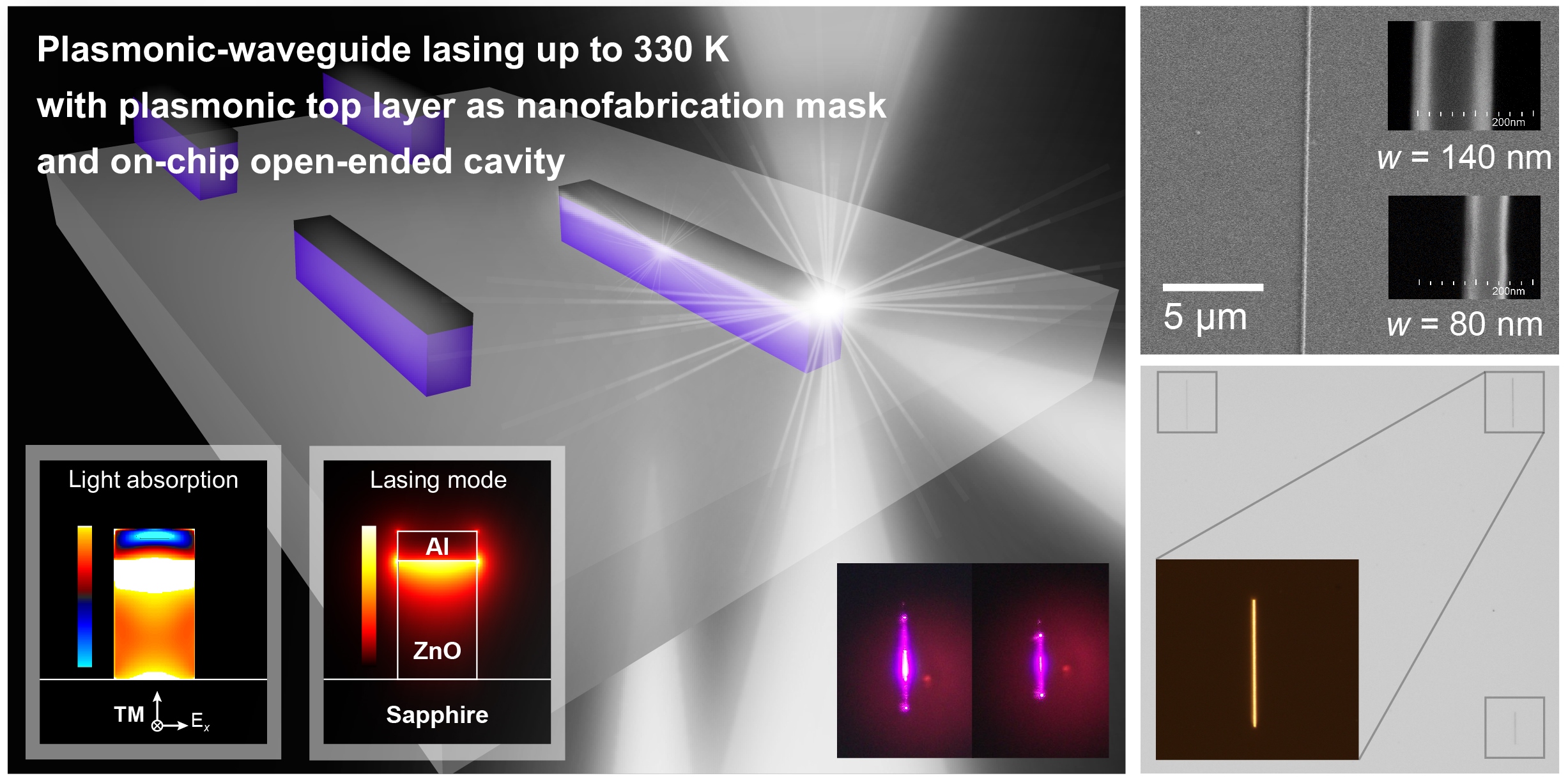
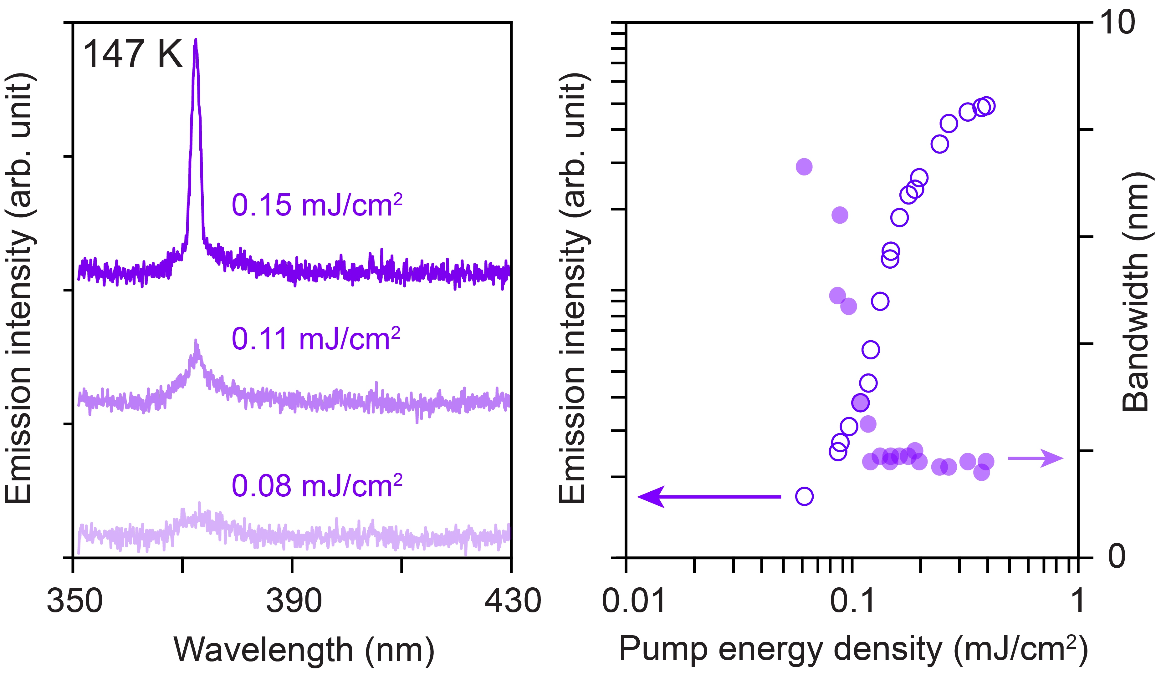
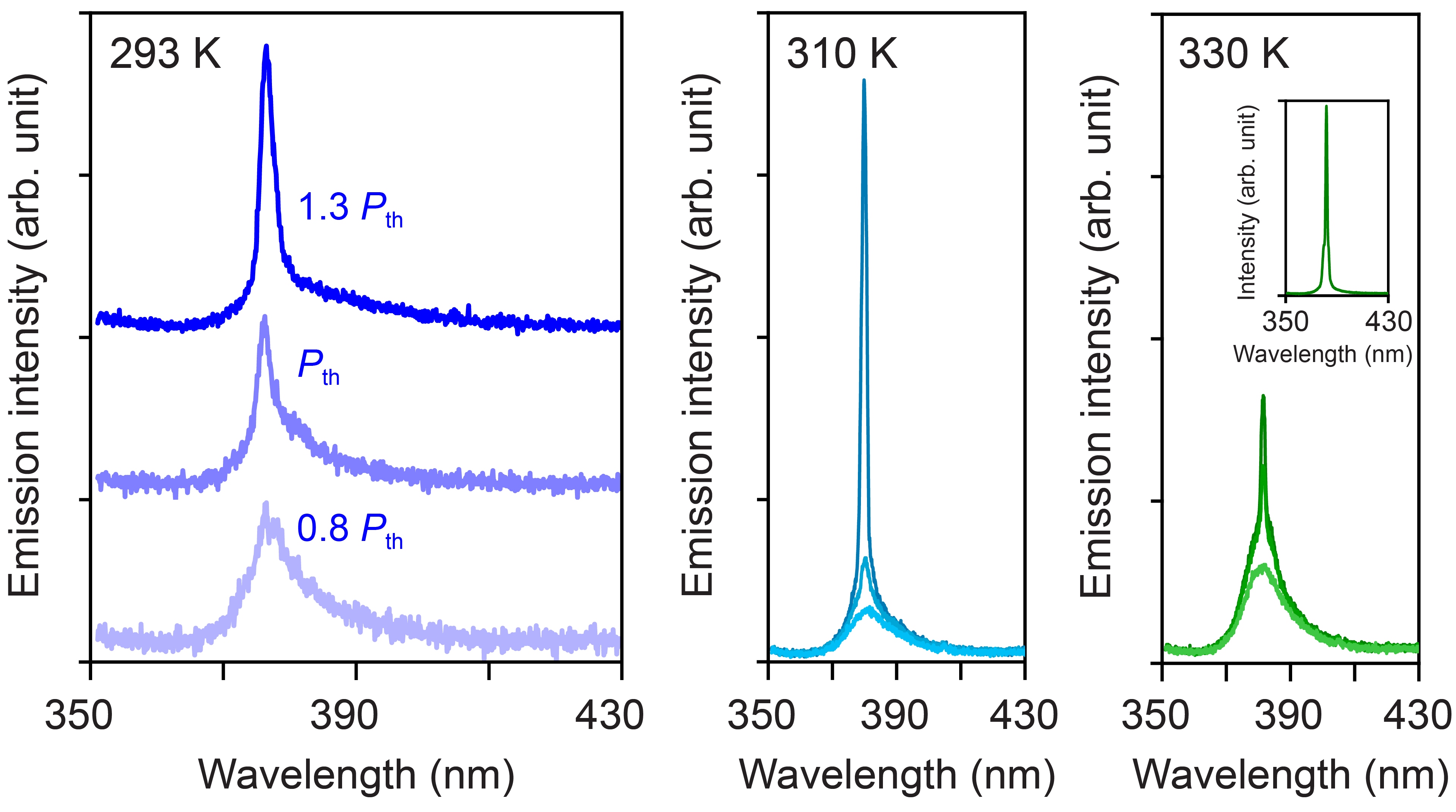
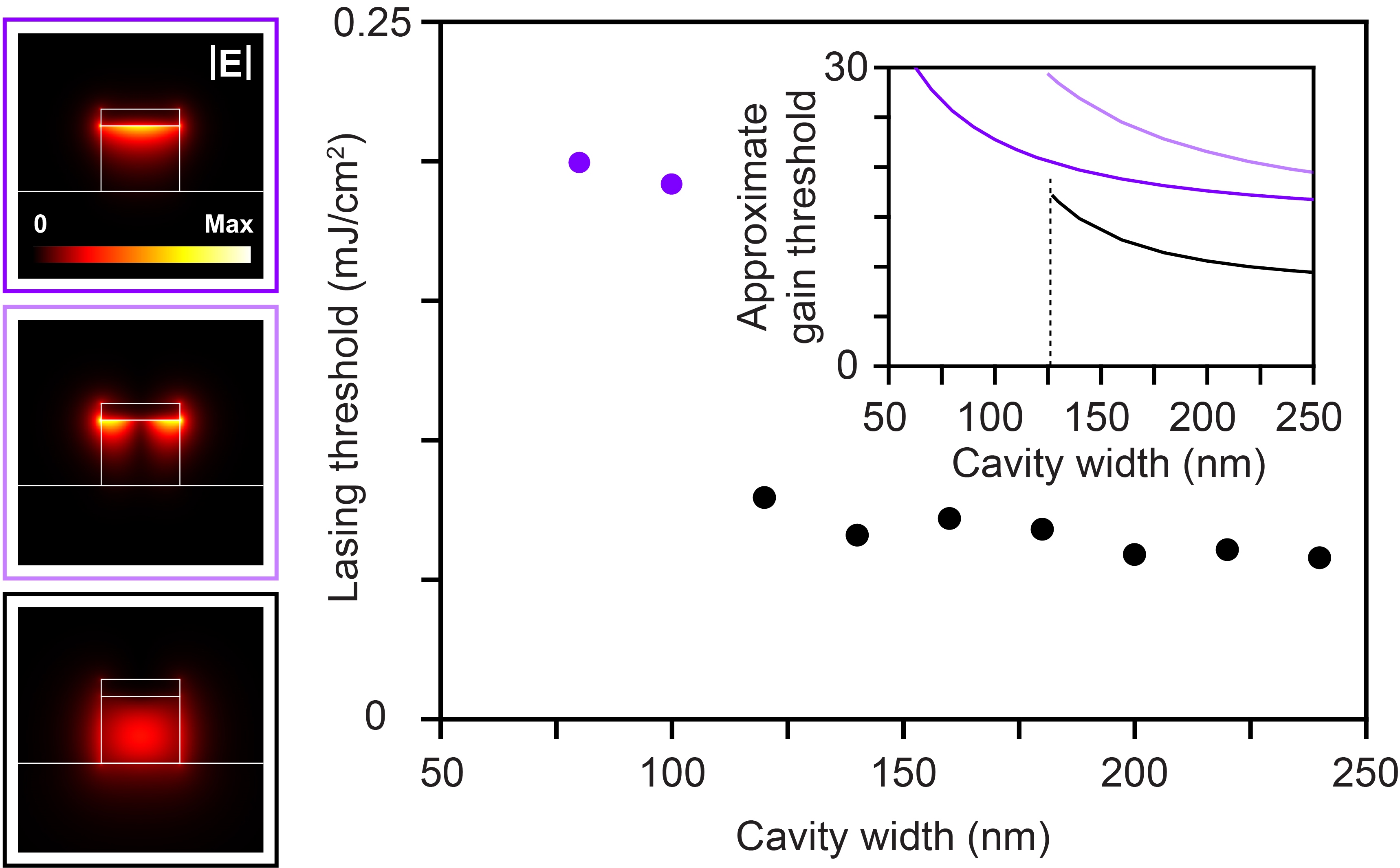
Plasmonic-waveguide lasers, which exhibit subdiffraction limit lasing and light propagation, are promising for the next-generation of nanophotonic devices in computation, communication, and biosensing. Plasmonic lasers supporting waveguide modes are often based on nanowires grown with bottom-up techniques that need to be transferred and aligned for use in optical circuits. Here, we demonstrate a monolithically fabricated ZnO/Al plasmonic-waveguide nanolaser compatible with the fabrication requirements of on-chip circuits. The nanolaser is designed with a plasmonic metal layer on the top of the laser cavity only, providing highly efficient energy transfer between photons, excitons, and plasmons, and achieving lasing in the ultraviolet region up to 330 K with a low threshold intensity (0.20 mJ/cm2 at room temperature). This work demonstrates the realization of a plasmonic-waveguide nanolaser without the need for transfer and positioning steps, which is the key for on-chip integration of nanophotonic devices.
Y.-L. Ho, J. K. Clark, A. Syazwan A. Kamal, J.-J. Delaunay, "On-Chip Monolithically Fabricated Plasmonic-Waveguide Nanolaser," NANO LETTERS, 18, 7769, 2018.
Plasmonic narrow-band thermal emitter
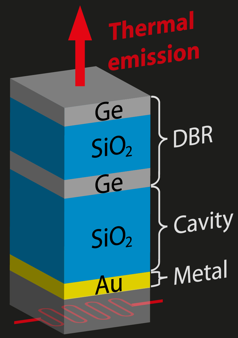
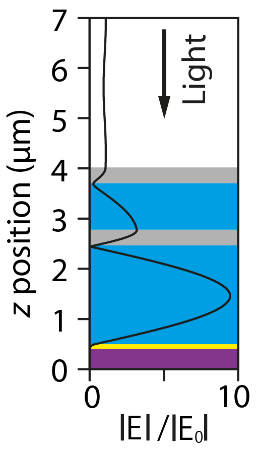
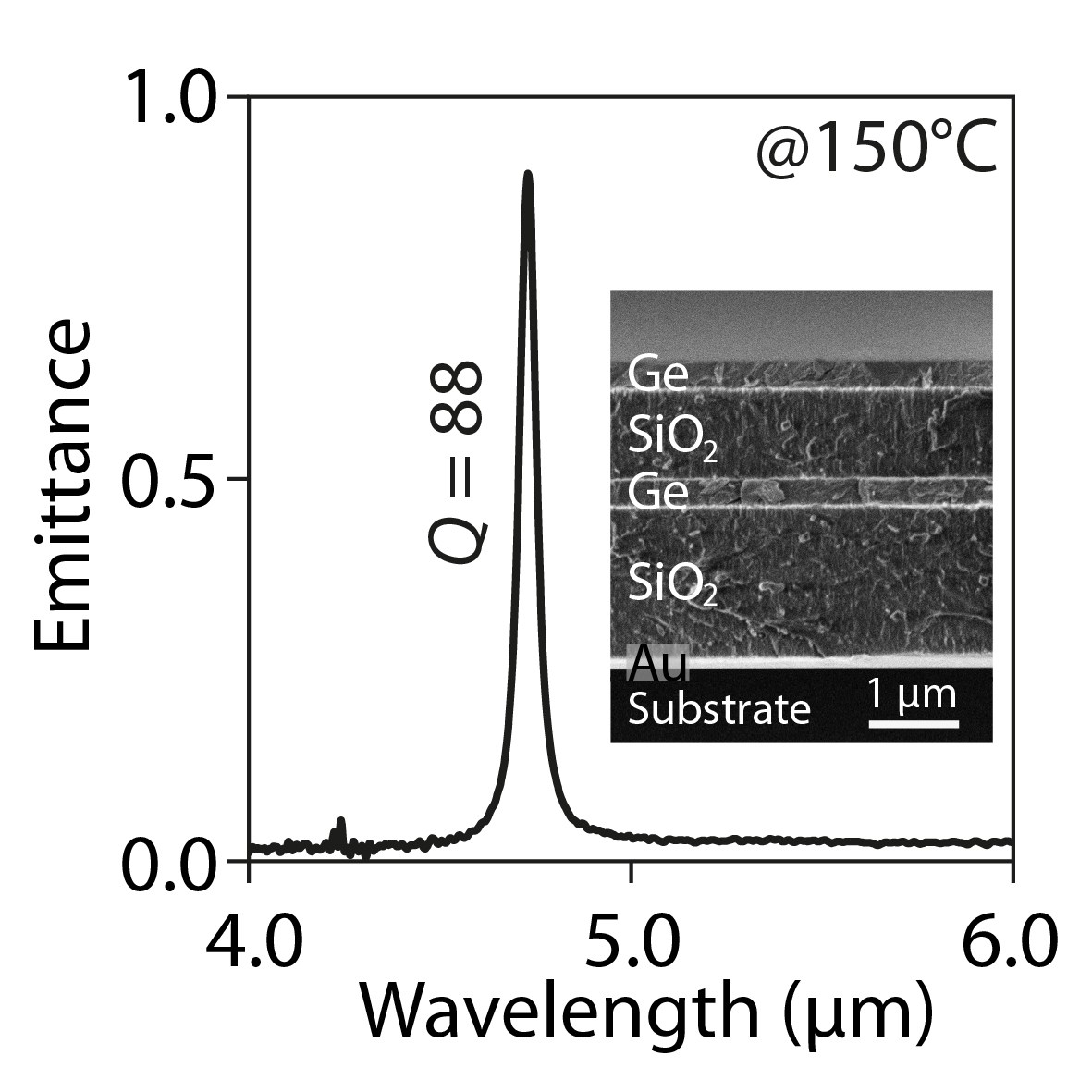
A hybrid structure that supports the coupling of a cavity mode and a Tamm plasmon (TP) mode is demonstrated as a spectrally selective thermal emitter. Unlike conventional TP structures, the presented hybrid structure contains an optical cavity sandwiched between the distributed Bragg reflector (DBR) and the metallic mirror of a typical TP structure. The TP-cavity hybrid structure exhibits a strong and sharp absorptance peak within a wide range of resonance wavelengths which can be realized by adjusting the cavity thickness. Upon heating, a strong and narrow-bandwidth thermal emittance peak is observed with a maximum emittance value of 0.90 and a resonance quality factor of 88 at a wavelength of 4.733 um (with background of 0.02 at 6 um). The Q-factor and the emittance peak to background ratio (45) of this structure are larger than those of any other reported SP- and TP-based thermal emitters. This easy-to-fabricate and high-performance infrared thermal emitter is ideal for applications where narrow-band infrared light sources are required.
Z. Wang, J. K. Clark, Y.-L. Ho, B. Vilquin, H. Daiguji, J.-J. Delaunay, “Narrow-band thermal emission realized through the coupling of cavity and Tamm plasmon resonances,” ACS PHOTONICS, 10.1021/acsphotonics.8b00236, 2018.
Solar water splitting with low external bias voltage
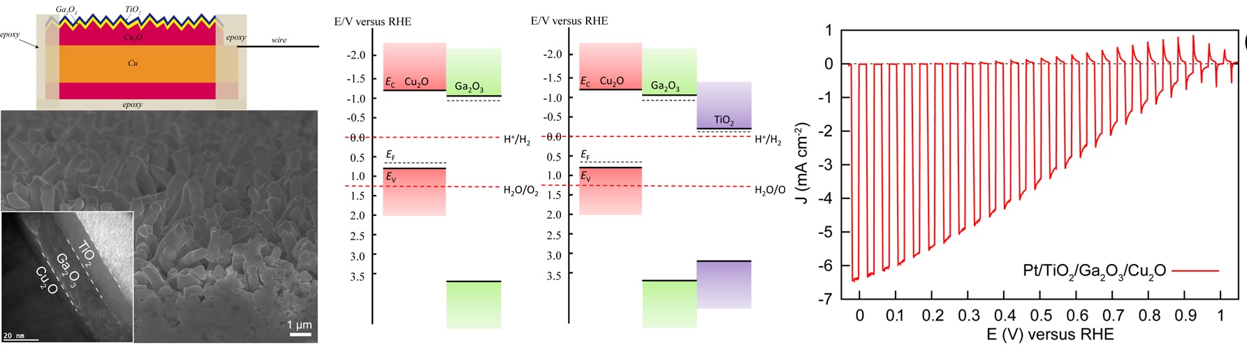
Coating n-type buffer and protective layers on Cu2O may be an effective means to improve the photoelectrochemical (PEC) water-splitting performance of Cu2O-based photocathodes. We examined the functions of the buffer layer and protective layer on Cu2O. It is found that a Ga2O3 buffer layer can form a buried junction with Cu2O, which inhibits Cu2O self-reduction as well as increases the photovoltage through a small conduction band offset between the two semiconductors. The introduction of a TiO2 thin protective layer not only improves the stability of the photocathode but also enhances the electron transfer from the photocathode surface into the electrolyte, thus resulting in an increase in photocurrent at positive potentials. These results show that the selection of overlayers with appropriate conduction band positions provides an effective strategy for obtaining a high photovoltage and high photocurrent in PEC systems.
C. Li, T. Hisatomi, O. Watanabe, M. Nakabayashi, N. Shibata, K. Domen and J.-J. Delaunay, “Positive onset potential and stability of Cu2O-based photocathodes in water splitting by atomic layer deposition of a Ga2O3 buffer layer,” Energy & Environmental Science 2015, 8, 1493-1500 (Highlighted as HOT Article in EES).
C. Li, T. Hisatomi, O. Watanabe, M. Nakabayashi, N. Shibata, K. Domen and J.-J. Delaunay, “Simultaneous enhancements in photovoltage and charge transfer of a Cu2O-based photocathode using a buffer and a protective layers,” Applied Physics Letters 2016, 109, 033902.
C. Li, Y. Li and J.-J. Delaunay, “A novel method to synthesize highly photoactive Cu2O microcrystalline films for use in photoelectrochemical cells,” ACS applied materials & interfaces 2013, 6, 480-486.
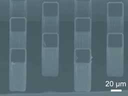
Plasmonic photocapacitor
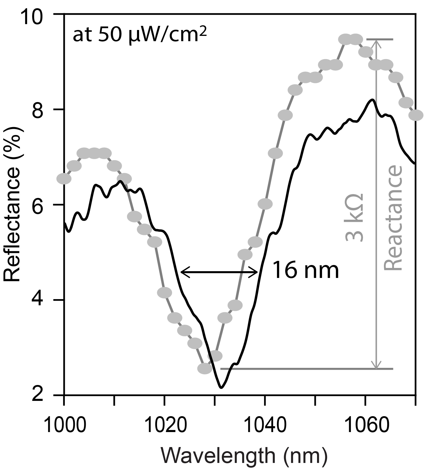
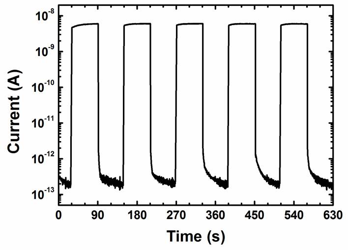
Interaction of light with metal sub-wavelength structures (hereafter nanostructures) has revealed new properties of light, such as light ability to pass through an array of nanoholes. Strong light confinement on the metal nanostructures in the form of a plasmon resonance was found to be at the origin of this far field property. Following this discovery, a wide variety of nanostructures have been studied and their optical responses have been used to monitor changes in their physical, chemical, and biological environments. The detection of this response in the far field is governed by the near-field properties of plasmon resonances. Although the plasmonic structures offer high performance in sensing, their micro integration on chips is difficult because of the readout in the far field. As such, structures that form an electrical micro-circuit and directly monitor the optical near-field variation without resorting to far-field optical detection would be more desirable. Here, we demonstrate an electronically readable photocapacitor based on a plasmonic nanochannel structure, which monitors the change in incident light wavelength with high spectral resolution and large impedance modulation. It is envisioned that an array of the plasmonic photocapacitors could be used to realize a miniaturized infrared spectrometric image-array-sensor.
Y.-L. Ho, L.-C. Huang and J.-J. Delaunay, “Spectrally Selective Photocapacitance Modulation in Plasmonic Nanochannels for Infrared Imaging,” NANO LETTERS, 16, 3094, 2016.
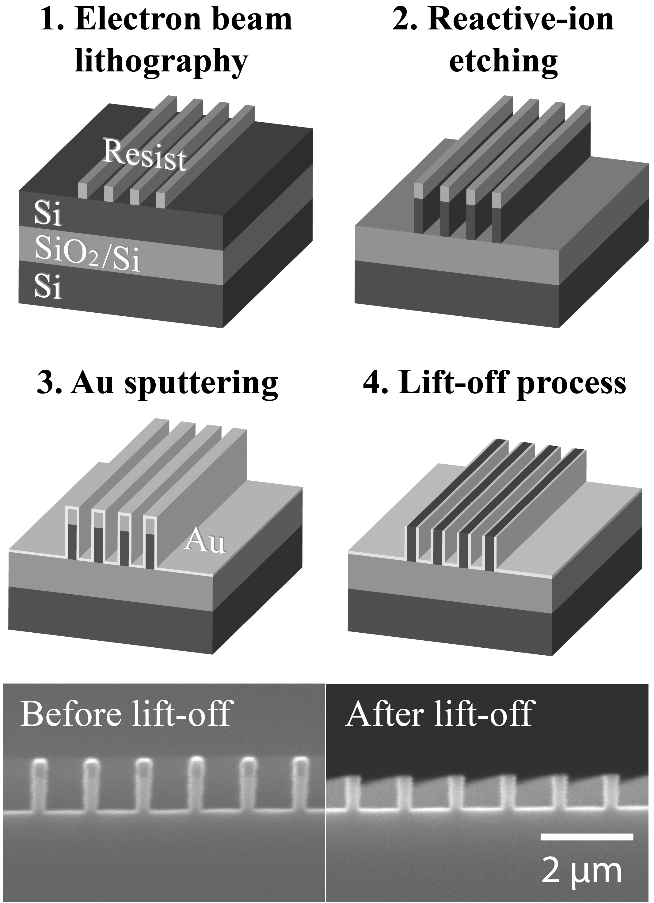
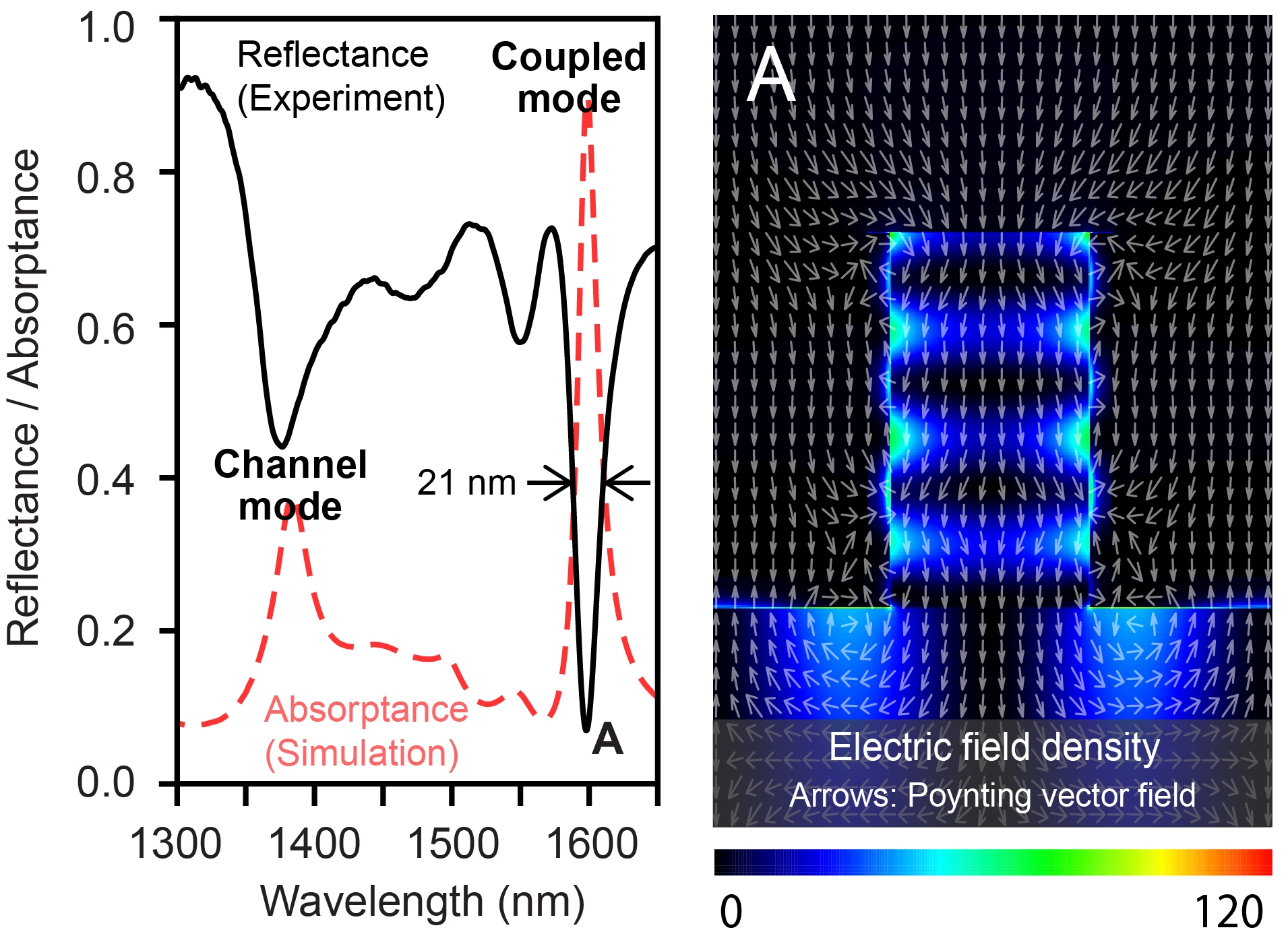
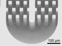
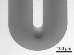
Plasmonics in nano-cavities for sensing
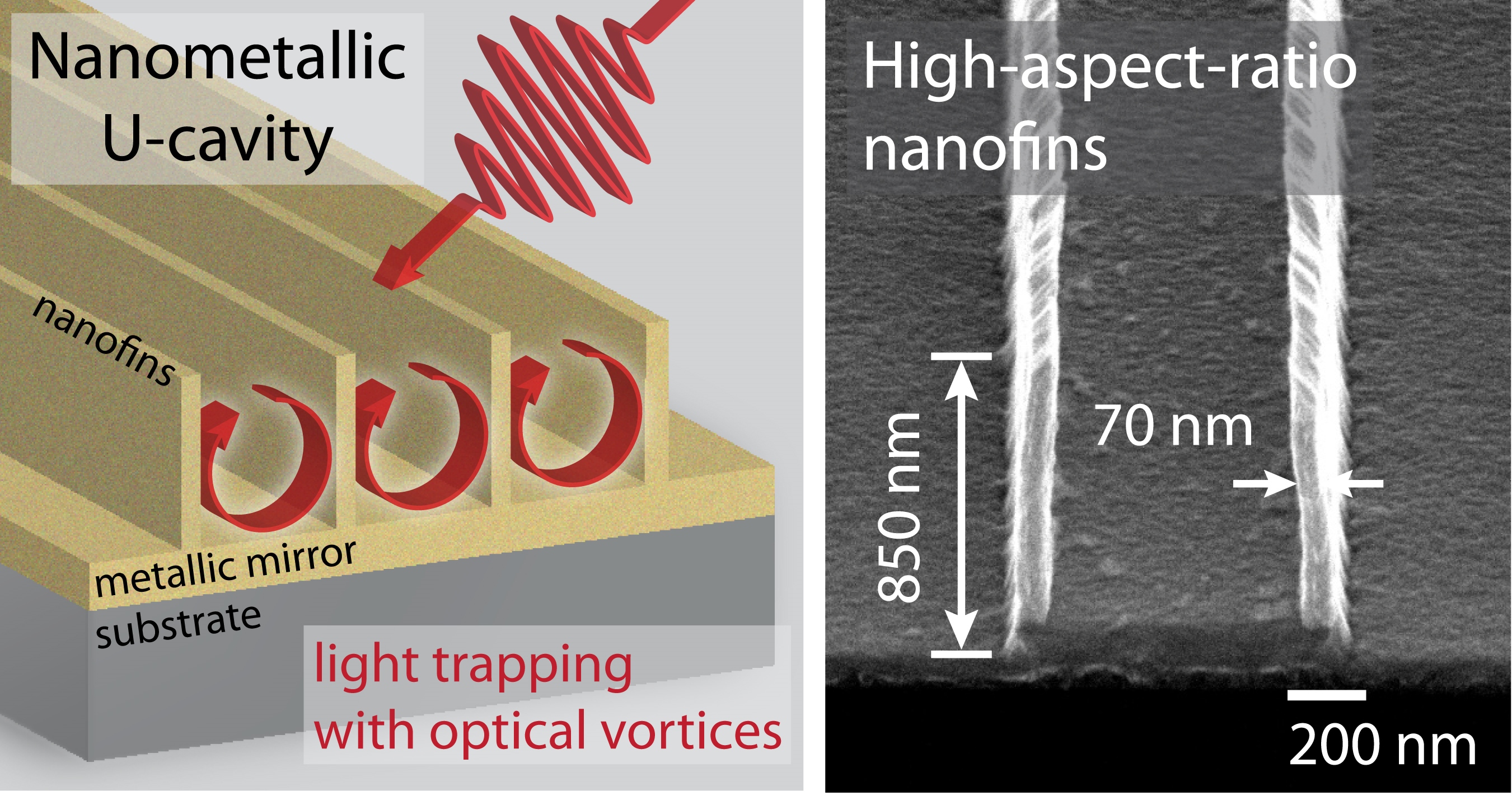
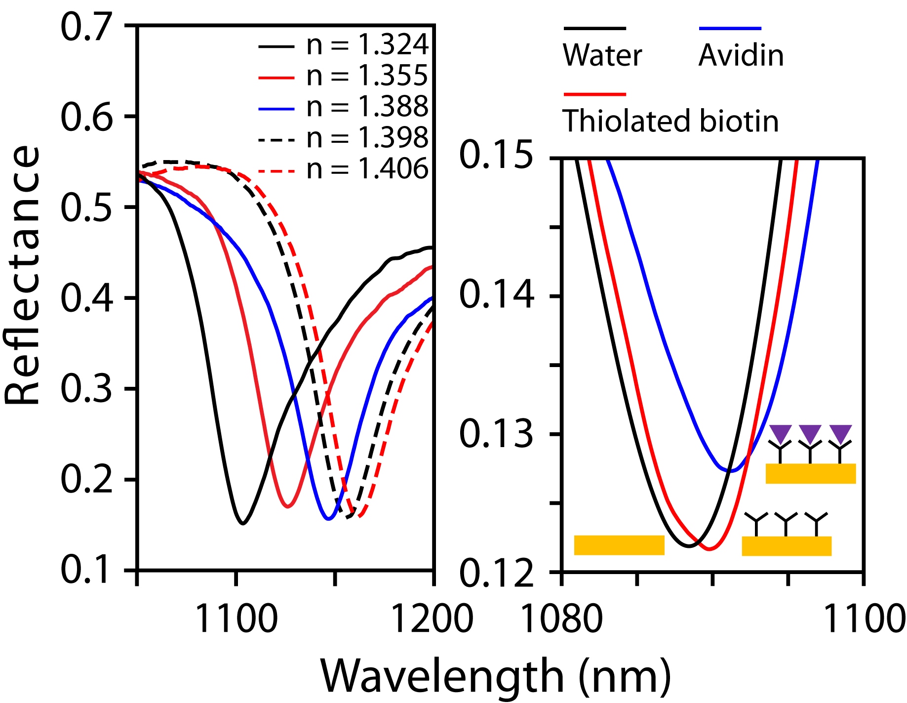
Perfect light confinement is achieved in high-aspect-ratio nanometallic U-shaped cavities through the coupling of the cavity ridge hot spots with scalable mirrored U-cavity resonances. Light is fully trapped in intense optical vortices and confined on the extended cavity surfaces, thus accumulating energy in tunable and strong resonances with narrow bandwidths and generating sensitive reflectance dips. The reflectance dip wavelength is readily controlled over a wide range of wavelengths covering the near-infrared region by varying the geometrical parameters of the U-cavities. The sensitivity of the reflectance dips to change in the surroundings is used to demonstrate biological sensing in a protein-ligand scheme. Thanks to the property of light trapping in the optical vortices, U-cavities have high potential for applications in various optical devices such as filters, transducers and switches.
Y.-L. Ho, A. Portela, Y. Lee, E. Maeda, H. Tabata, and J.-J. Delaunay, “Hollow plasmonic U-cavities with high-aspect-ratio nanofins sustaining strong optical vortices for light trapping and sensing,” ADVANCED OPTICAL MATERIALS, 2014. (DOI: 10.1002/adom.201400145)
Y.-L. Ho, Y. Lee, E. Maeda, and J.-J. Delaunay, “Coupling of localized surface plasmons to U-shaped cavities for high-sensitivity and miniaturized detectors,” OPTICS EXPRESS, 21, 1531, 2013.
E. Maeda, Y. Lee, Y. Kobayashi, A. Taino, M. Koizumi, S. Fujikawa and J.-J. Delaunay, “Sensitivity to refractive index of high-aspect-ratio nanofins with optical vortex,” NANOTECHNOLOGY, Vol. 23, 505502, 2012.
Water splitting with sun light using nanowires
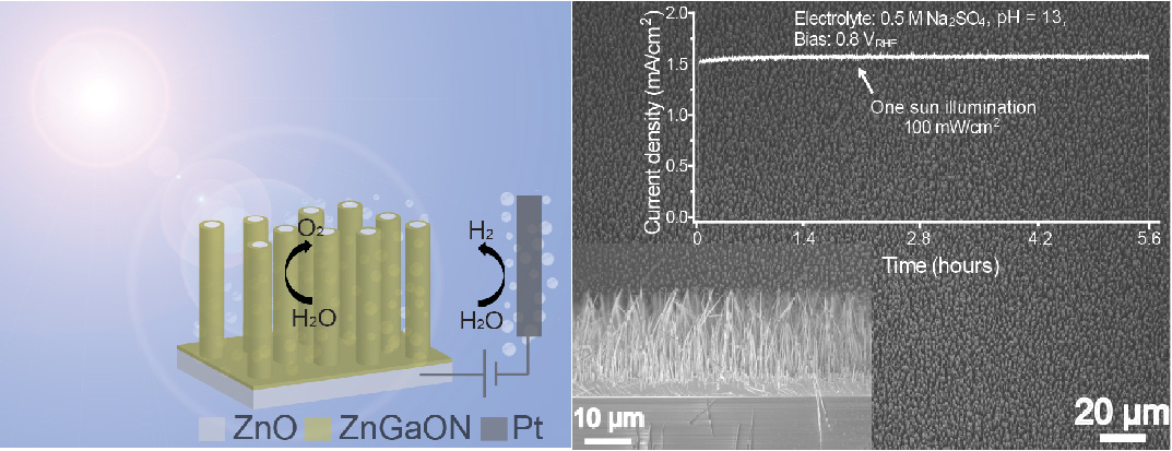
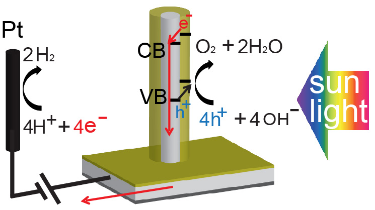
Efficient and stable water splitting into hydrogen and oxygen with sun light is realized on a hybrid photo-electrode consisting of semiconducting nanowire-on-a-film structure. Conventional photo-electrodes are in the form of a bulk film or a layer of nanostructures and, therefore, have limited efficiency caused by the film small area or the nanostructure layer poor conduction. Thus, a hybrid type of photo-electrode with properties of both nanostructures and films is needed. The synthesized photo-anode consisting of core-shell ZnO-ZnGaON nanowires connected at their roots to a single crystalline ZnO film achieved stable water splitting without resorting to co-catalyst.
M. Zhong, Y. Ma, P. Oleynikov, K. Domen and J.-J. Delaunay “Conductive ZnO-ZnGaON nanowire-array-on-a-film photoanode for stable and efficient sunlight water splitting,” ENERGY & ENVIRONMENTAL SCIENCE, (DOI: 10.1039/C3EE43806F) 2014.
M. Zhong, Y. Li, I. Yamada, J.-J. Delaunay, “ZnO-ZnGa2O4 core-shell nanowire array for stable photoelectrochemical water splitting,” NANOSCALE, Vol. 4, 1509, 2012.
M. Zhong, Y. Sato, M. Kurniawan, A. Apostoluk, B. Masenelli, E. Maeda, Y. Ikuhara and J.-J. Delaunay, “ZnO dense nanowire array on a film structure in a single crystal domain texture for optical and photoelectrochemical applications,” NANOTECHNOLOGY, Vol. 23, 495602, 2012.
Light concentration in gold short nanosphere chain on platinum mirror for surface-enhanced Raman scattering
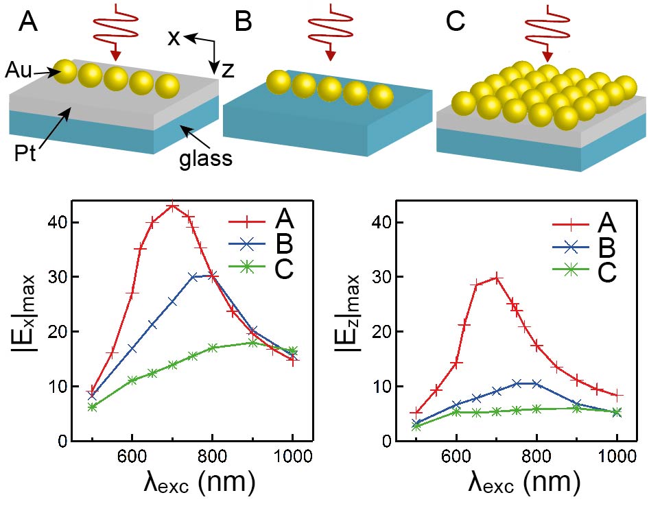
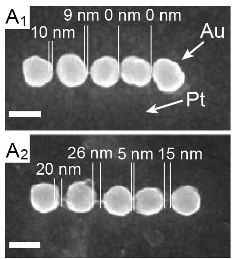
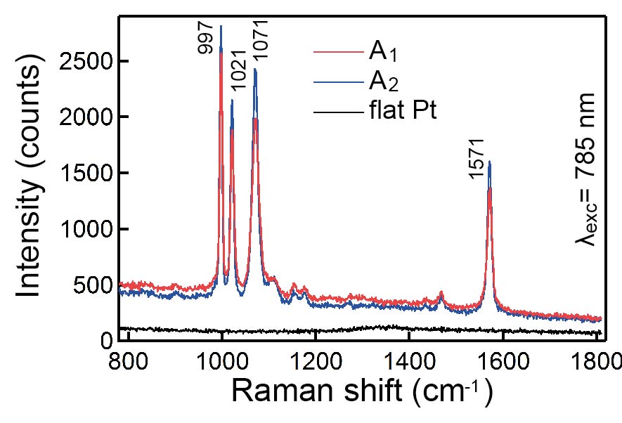
We studied closely spaced gold nanosphere chains on Pt mirrors exhibiting strong plasmon coupling between both horizontally and vertically oriented modes relative to the chain. Thanks to the effective light concentration, the short nanosphere chain demonstrated strong surface enhanced Raman scattering.
Yaerim Lee, Minoru Abasaki, Alejandro Portela, Jean-Jacques Delaunay, "Effective light concentration in gold short nanosphere chain on platinum mirror for surface-enhanced Raman scattering," Applied Physics Letters, 105, 121114, 2014.
Nanowires for photon detection / 金属酸化物半導体ナノワイヤを用いた太陽光ブラインド紫外線センサ
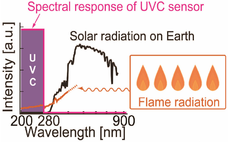
We develop methods to assemble nanowires into functional devices such as light detectors. We proposed to bridge ZnO nanowires between self-grown ZnO electrodes to fabricate an ultra-high sensitivity ultraviolet photodetectors. This fabrication method is amenable to production on a large scale and at an effective cost. Recently, we demonstrated solar-blind photodetection with bridged gallium oxide nanowires.
本研究の目的は,金属酸化物半導体ナノワイヤを用いることにより,太陽光ブラインド紫外線センサを高感度化することである.近年,炎や放電現象の検知器,紫外線スイッチ,ミサイル防衛システムなどに利用するため,波長がおよそ280 nm以下の光である太陽光ブラインド紫外線(Solar-blind UV)を検出するセンサへの需要が高まっている.地表における太陽光には280 nm以下の波長の光は含まれないため,このセンサを用いることによって,太陽光の影響を受けない検知が可能になる.
本研究では,減圧CVD(化学気相成長)法によりナノワイヤを作製する.減圧CVD法は,電気炉で減圧して加熱気化させた試料を基板上に蒸着させる方法である.圧力・ガス種・ガス流量・温度・温度勾配・時間・材料量等のパラメータを変化させ,ナノワイヤの組成と構造を制御する.当研究室では,現在までに金属酸化物半導体であるZnOを用いてナノワイヤを作製し,紫外線に反応する素子を開発することに成功した.
Y.B. Li, F. Della Valle, M. Simonnet, I. Yamada, J.-J. Delaunay, "High-performance UV detector made of ultra-long ZnO bridging nanowires," NANOTECHNOLOGY, Vol. 20, 4, 045501, 2009.
Y.B Li, T. Tokizono, M. Liao, M. Zhong, Y. Koide, I. Yamada, J.-J. Delaunay, “Efficient Assembly of Bridged Ga2O3 Nanowires for Solar-blind Photodetection,” ADVANCED FUNCTIONAL MATERIALS, Vol. 20, 3972, 2010.
パラジウムホールアレイを用いたガスセンサ
1998年,Ebbesenらによって発見されたExtraordinary Optical Transmission (EOT)を応用した水素センサーを研究している.これまでの研究によって,世界 初のEOTを応用した光学式水素センサーの開発に成功した.このセンサーは光学 式水素センサーの中では屈指の性能を有している.
EOTとは,金属サブ波長開口配列上の表面プラズモンによって,特定波長の透 過光が増幅される現象である.透過スペクトルは,開口配列の構造・誘電率に影 響される.本研究では,開口配列の材料に水素吸蔵金属であるパラジウムを用い ることで,水素センシングを可能とした.パラジウムは水素を吸収した際に,金 属結晶構造が変化し,誘電率の低下を生じる.この現象により,EOTのスペクト ルが変化し,水素の吸蔵状態を予測することができる.研究室では,実験・光学 シミュレーションの双方から,この水素センサーの特性を分析評価している.
現在は,水素以外のガス種を検知するセンサーの開発にも取り組んでいる.
E. Maeda, S. Mikuriya, K. Endo, I. Yamada, A. Suda, J.-J. Delaunay, "Optical hydrogen detection with periodic subwavelength palladium hole arrays," APPLIED PHYSICS LETTERS, Vol. 95, 13, 133504, 2009.
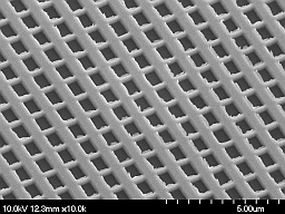
マイクロ ガスクロマトグラフィ
MEMS技術を用いてガスクロマトグラフ装置(GC)をシリコンチップ上に実現するマイクロGCの研究が行われているが,中でも,分析速度向上をめざして,できるだけ長さが短く分離効率の高いマイクロGCカラムの実現が期待されている.3次元構造を持つカラムは分離効率を向上させるが,複雑な3次元構造を持つカラム内に,ガス分離機能を果たす固定相を均一に塗布することは困難であった.
本研究では,コンフォーマルに塗布できるパリレン材料を固定相に用いることを提案した.具体的には,パリレン材料であるdiX NおよびdiX AMを固定相として塗布した3次元構造マイクロGCカラムを作製し,ガス分離実験によって評価して,パリレン材料が固定相として利用可能であることを示した.
T. Nakai, S. Nishiyama, M. Shuzo, J.-J. Delaunay, I. Yamada, "Micro-fabricated semi-packed column for gas chromatography by using functionalized parylene as a stationary phase," JOURNAL OF MICROMECHANICS AND MICROENGINEERING, Vol. 19, 6, 065032, 2009.
レーザ回折トモグラフィ顕微鏡
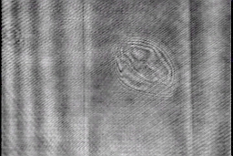
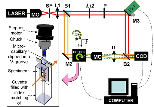

多くの生体組織は,半透明の物体である.半透明の物体は位相物体と呼ばれる. 位相物体とは,光を照射した際,光の強度が変化せず,光の位相が変化する物体を指す. 本研究では,位相物体による光の回折を,干渉縞によって捉え,生体組織の3次元位相情報を取得すること(トモグラフィ)に成功した.
S. Vertu, J.-J. Delaunay, I. Yamada, O. Haeberle, "Diffraction microtomography with sample rotation: influence of a missing apple core in the recorded frequency space," CENTRAL EUROPEAN JOURNAL OF PHYSICS, Vol. 7, 1, pp.22-31, 2009.
ZnOナノ・マイクロ構造を用いたガスセンサ
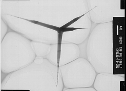
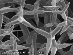
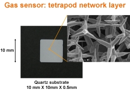
ZnOなどの金属酸化物半導体は,ガス成分との反応により電気抵抗が変化するため,ガスセンサとして用いることができる.このとき,ナノ・マイクロ構造を持った材料を用いると比表面積が増大し,ガス成分との反応による電気抵抗変化も大きくなるので,ガスセンサの高感度化が期待できる.本研究では,ZnOナノ・マイクロ構造を合成し,ppbオーダのガスを検知可能な高感度ガスセンサの実現をめざしている.
CVD法や液相成長法を用いて,テトラポッド型やフラワー型ZnOを合成するとともに,これにプラズマ表面処理を行って微細な凹凸を生じさせ,比表面積の更なる増加に成功した.これらのZnOマイクロ・ナノ構造を材料としてガスセンサを作製し,1ppmのエタノールガスを検知することに成功した.
J.-J. Delaunay, N. Kakoiyama, I. Yamada, "Fabrication of three-dimensional network of ZnO tetratpods and its response to ethanol," MATERIALS CHEMISTRY AND PHYSICS, Vol. 104, 1, pp.141-145, 2007.